
AI Executive Summary
"This article analyzes the critical transition from organic to glass substrates in semiconductor packaging to bypass the physical reticle limit. It highlights the strategic importance of material science in enabling the next generation of hyper-scale AI hardware."
The semiconductor industry has hit a physical wall called the reticle limit. For decades, the maximum size of a single chip has been capped at roughly 858 square millimeters, a constraint imposed by the aperture of the lithography machines that print the circuits. When an AI processor needs more transistors than this area allows, engineers have traditionally relied on chiplets, stitching multiple smaller dies together on an organic substrate. But this approach is failing as the scale of generative AI demands packages that dwarf the original reticle size, leading to catastrophic warpage and signal degradation.
Why does the substrate matter if the silicon is the brain? The substrate is the foundation that connects the chip to the rest of the system, and current organic materials—mostly plastic-based resins like Ajinomoto Build-up Film (ABF)—are simply too flexible. As packages grow larger to accommodate more HBM (High Bandwidth Memory) and logic dies, these organic bases bend under the heat of operation. This warpage creates microscopic gaps in the solder bumps, leading to intermittent failures or total system collapse in high-performance computing environments.
The Failure of Organic Foundations
Organic substrates suffer from a fundamental mismatch in the Coefficient of Thermal Expansion (CTE). Silicon expands very little when it gets hot, but plastic substrates expand significantly. In a massive AI package, this tug-of-war between the rigid silicon and the expanding plastic creates immense mechanical stress. This stress doesn't just risk physical cracks; it limits how densely we can pack the interconnects. If you place the connections too close together, the thermal expansion will literally rip the wires out of the substrate.
Does this mean we just accept slower chips? No, but it means the industry must change the material of the floor itself. The current reliance on organic materials has forced designers into a corner where they must choose between package size and reliability. To break the reticle limit and move toward 'system-on-package' designs that exceed 100mm x 100mm, the industry needs a material that behaves more like silicon and less like plastic.
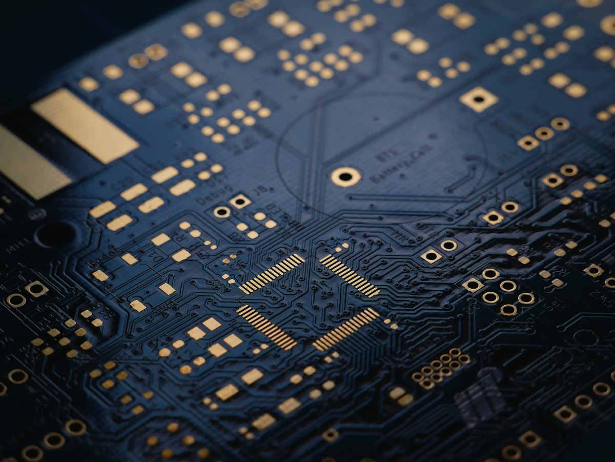
This material struggle is most evident in the latest generation of GPU clusters deployed across North American and European data centers. These systems are pushing power envelopes toward 1,000 watts per socket, generating heat that makes organic substrate instability a primary cause of yield loss. When a substrate warps by even a few microns across a large surface, the precision required for micro-bumps is lost, rendering an expensive piece of silicon useless.
The industry is now looking toward glass. Unlike organic resins, glass can be engineered to have a CTE that almost perfectly matches silicon. This synchronization means that as the chip heats up, the substrate and the silicon expand at the same rate, virtually eliminating the mechanical stress that causes warpage. This stability allows for much larger packages, effectively bypassing the reticle limit by enabling the integration of far more chiplets on a single, flat plane.
The Mechanics of the Silica Shift
Glass isn't just about stability; it is about precision. Glass substrates allow for Through-Glass Vias (TGVs), which are holes drilled through the material to create vertical electrical connections. Because glass is so much stiffer and smoother than organic materials, these vias can be made significantly smaller and spaced closer together. This increases the interconnect density by orders of magnitude, allowing for faster data transfer between the processor and the memory.
Consider the implications for power delivery. Organic substrates require thick copper layers to carry high currents, which further contributes to warpage. Glass can support higher-density routing and integrated capacitors, bringing power closer to the silicon die. This reduces the voltage drop and increases the energy efficiency of the entire package, a critical requirement for the next generation of trillion-parameter models.
| Property | Organic (ABF) | Glass Substrate |
|---|---|---|
| Thermal Expansion (CTE) | High (Mismatched) | Low (Matched to Silicon) |
| Surface Roughness | Moderate | Ultra-Low/Atomic |
| Warpage Risk | High at Large Scales | Minimal |
| Interconnect Density | Limited by Pitch | High (TGV enabled) |
| Max Package Size | Constrained | Significantly Expanded |
The transition to glass is not without risk. Glass is inherently brittle, and the processes used to handle it in a fab are entirely different from those used for plastics. One wrong move in the handling chain can lead to a shattered substrate, destroying everything mounted upon it. Furthermore, the industry must develop new ways to bond copper to glass, as the chemical adhesion properties differ wildly from those of organic resins.
Despite these risks, the reward is a total decoupling of chip size from the reticle limit. By using glass, chipmakers can build 'super-packages' that act as a single giant chip, containing multiple compute dies and massive pools of memory without the fear of physical deformation. This allows for a level of integration that was previously thought to be a decade away.
"The move to glass is not an incremental improvement; it is a fundamental change in the physics of how we connect silicon to the world."— Lead Packaging Engineer, Advanced Compute Division
This shift is already triggering a reorganization of the supply chain. We are seeing a convergence between the semiconductor industry and the high-end glass industry, with companies in Japan and the United States racing to standardize TGV manufacturing. The ability to mass-produce glass substrates with zero defects will likely become the next great competitive moat in the AI hardware race.
Systemic Implications for Global Compute
What happens when the reticle limit no longer dictates the size of a processor? We enter the era of the 'Modular Giant.' Instead of fighting to squeeze every single transistor into a single die, designers will optimize for the most efficient chiplet size and simply tile them across a massive glass plane. This reduces the cost of manufacturing, as smaller dies have higher yields than massive, complex ones.
This change will be felt most acutely in the edge-computing clusters of East Asia and the massive data centers of the American Midwest. The ability to deploy larger, more efficient processors means that the physical footprint of AI training can be reduced while increasing the total compute density. We are moving from a world of 'chips on boards' to a world of 'systems on glass.'

Ultimately, the bet on glass is a bet on the continued growth of AI. If the demand for compute had plateaued, the industry would have continued to tweak organic substrates. But the appetite for intelligence is insatiable, and the physics of plastic can no longer keep up. Glass provides the structural integrity and electrical precision required to scale the hardware to match the software's ambition.
The transition will be messy and expensive, but the alternative is stagnation. Those who master the glass substrate will control the physical limits of artificial intelligence, deciding exactly how large and how fast the next generation of machines can actually be.